Synopsys.ai AI-Powered EDA Suite Accelerates Chip Design and Cuts Costs
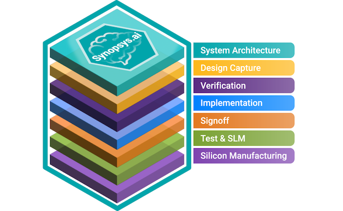
Synopsys has introduced the industry's first full-stack AI-powered suite of electronic design automation tools that covers all stages of chip design, from architecture to design and implementation to manufacturing. The Synopsys.ai suite promises to radically reduce development time, lower costs, improve yields, and enhance performance. The set of tools is set to be extremely useful for chips set to be made on leading-edge nodes, such as 5nm, 3nm, 2nm-class, and beyond.
Chip Design Challenges
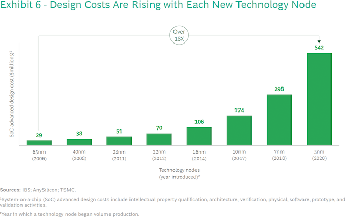
As chips gain complexity and adopt newer process technologies, their design and manufacturing costs escalate to unprecedented levels. Designing a reasonably complex 7 nm chip costs about $300 million (including ~ 40% for software). In contrast, the design cost of an advanced 5 nm processor exceeds $540 million (including software), according to International Business Strategies (IBS) estimates. At 3 nm, a complex GPU will cost about $1.5 billion to develop, including circa 40% for software.
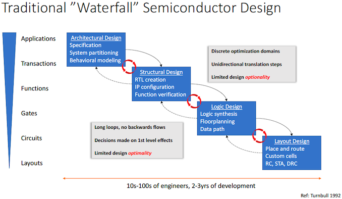
The traditional 'waterfall' semiconductor design approach is perhaps one of the reasons why chip development costs skyrocket so rapidly. It takes hundreds (if not thousands) of engineers and thousands of servers over several years to develop and simulate architectural, structural, logic, and layout designs. Meanwhile, every design stage involves tasks that are essential for the quality of the chip, but they are iterative and time-consuming in nature. For obvious reasons, as chips get more complex, each design change gets longer as companies cannot throw in as many engineers as they want to a given task because the number of people they have is limited.
Things get more challenging as the waterfall approach almost excludes backward flows, so people implementing one of the thousands of possible place and route designs have little to zero influence on the architectural or structural design. As a result, the only way to avoid inefficiencies resulting in higher-than-expected costs, lower-than-expected performance, and/or higher-than-expected power consumption is to make different design teams work closer together at all stages. Yet, this gets harder as design cycles get longer.
Manufacturing costs at 5 nm and 3 nm production nodes are also noticeably higher than those on previous-generation fabrication technologies. The latest leading-edge manufacturing processes extensively use extreme ultraviolet lithography and more expensive raw materials (e.g., pellicles for photomasks, resists, etc.). Therefore, it gets even more crucial for chip developers to build close-to-perfect designs that are cheaper to make.
In general, the semiconductor industry faces several challenges these days as it needs to cut down development time, maintain (or even reduce) chip development costs, and ensure predictable manufacturing costs. Everything has to be done when the industry faces a deficit of highly skilled engineers.
This is where the Synopsys.ai EDA suite comes into play.
From Scratch to High-Volume Manufacturing
The Synopsys.ai full-stack EDA suite consists of three key applications the DSO.ai AI for chip design: the Synopsys VSO.ai for functional verification, and the TSO.ai for silicon test. The suite is designed to speed up iterative and time-consuming chip design stages using machine learning and reinforcement learning accelerated by modern CPUs and GPUs.
Synopsys has been offering its DSO.ai place and route AI-driven solution for about two years now, and over 100 designs have been taped out using the EDA tool so far. But this time around, the company is looking at fast-tracking all design stages with AI. The software suite can be used at all stages, including simulations, design capture, IP verification, physical implementation, signoff, test, and manufacturing.
Better Architectures Delivered Faster
Small groups of very talented engineers typically develop microarchitectures, and this stage is considered by many as an intersection of technology and art. In fact, microarchitectures are developed fairly quickly too. Synopsys says that even this stage can be accelerated and improved with AI as artificial as, unlike people, machines can quickly estimate the most efficient architecture parameters and data paths.
The General Manager of Synopsys's Electronic Design Automation Group (EDA), Shankar Krishnamoorthy, states, "The whole process of developing a chip starts with the architecture of the chip and there are a lot of decisions to be made there," He also went on to say "How big does your cache need to be? What kind of interfaces run between your computer and memory? What configurations of memory should you consider, so there are many, many choices there, which an architecture expert would explore rapidly, and then converge on what are the right parameters to implement the chip with. So that process itself is something where AI can be used to rapidly explore that solution space […] and produce an even better result that they may not have gotten to, just because of the compute power that AI can work with."
Another aspect of using AI for microarchitectural explorations is boosting the microarchitecture development capabilities of a given company amid shortages of experienced architects.
Shankar Krishnamoorthy also said, "In cases when you have an expert architect already there, AI is really an assistant. The modern AI techniques are really good at zooming in on the spaces of interest in a very large parameter space by using rewards and penalties. Then you [end up with] a set of menu of choices (such as tradeoffs between power and performance) from which the architect sort of picks the best one for the workload of interest."
Speeding Up IP Verification
Functional and IP verification is a chip design step that takes up a lot of time. It is imperative to test each IP individually and ensure that it functions correctly before integrating them, as the complexity of verification increases exponentially when multiple IPs are combined. Meanwhile, it is crucial to achieving a high level of test coverage for each individual IP.
Nowadays, the common approach for verifying IP involves the designer creating a test benchmark that reflects their verification strategy. This test benchmark is then simulated using conventional simulation techniques, such as constrained random simulation, with the help of a traditional simulator. Achieving high target coverage for a given IP faster is a challenge that can be addressed by the Synopsys VSO.ai, which is part of Synapsys.ai.
"By embedding techniques like reinforcement learning deep into the simulation engine, you can achieve that target coverage" said the head of Synopsys's EDA group. "You say, I need 99% coverage of this IP, you can achieve that target coverage in a much shorter period of time, and using much fewer simulations, because essentially, that reinforcement learning engine that is embedded into the simulation engine is constantly [communication] with the engine that is generating the stimulus."
Renesas confirmed that the Synapsys VSO.ai software could both expand target coverage and speed up the IP verification process.
Takahiro Ikenobe, who is the IP Development Director of the Shared R&D Core IP Division at Renesas, said, "Meeting quality and time-to-market constraints is fast becoming difficult using traditional human-in-the-loop techniques due to the ramp in design complexity. Using AI-driven verification with Synopsys VSO.ai, part of Synopsys.ai, we have achieved up to 10x improvement in reducing functional coverage holes and up to 30% increase in IP verification productivity demonstrating the ability of AI to help us address the challenges of our increasingly complex designs."
Place and Route Done Fast
Speaking of increasingly complex designs, we must remember how hard it is to realize the modern processor's design physically. While modern EDA tools streamline chip development, skilled human engineers are still required to efficiently implement chip floorplan, layout, placement, and routing, utilizing their experience to create efficient designs. Although experienced engineers typically work fast, they are limited in their ability to evaluate hundreds of design options, explore all potential combinations, and simulate tens or even hundreds of different layouts to identify the optimal design within a reasonable timeframe. As a result, in many cases, they implement their best-known methodologies, which may not be the most efficient ones for a particular chip made on a particular production node.
This is when they can use the Synopsys DSO.ai platform that does not need to simulate all the possible ways to place and route a chip but leverages artificial intelligence to evaluate all combinations of architectural choices, power and performance targets, geometries and then simulate a few different layouts to find the one that complies with desired performance, power, area, and cost (PPA) combination in a fraction of the time.
Speaking of simulation, it is important to note that simulating a physically large chip (whether a CPU, GPU or a memory IC) is rather hard to accomplish. Traditionally chip designers used large machines based on CPUs or FPGAs to simulate future chips. Still, recently Synopsys applied GPU acceleration for these workloads and got a several-fold performance uplift.
"If we look at the design of discrete memory, like DRAM or NAND flash, these are very large circuits that need to be simulated for electrical correctness, physical correctness, you know, stress, IR drop all the other types of effects," Krishnamoorthy told us. "Simulation of these very large discrete memory structures is very time-consuming. That's an area where we have successfully applied GPU acceleration in order to achieve several-fold acceleration of the time it takes to simulate these large circuits."
One of the interesting things that Synopsys mentioned during our conversation is that the DSO.ai tool can be used to implement analog circuits — which barely (if at all) scale with each new node — in accordance with new design rules.
"Fundamentally, if you take a PLL, or you take any other type of analog circuit, and you are really not changing the circuit itself, you are migrating it from, let's say, 7 nm to 5 nm or 5 nm to 3 nm," explained the Synopsys executive. "That process of migrating a circuit from one node to another is something that is ripe for automation and ripe for the application of AI. So that is another area where we have applied AI to accelerate that process and cut down the effort and time needed to migrate analog circuits by a significant amount."
According to Synopsys, comparable AI capabilities can simplify the task of transferring chip designs between diverse foundries or process nodes. However, it is worth considering that intricate designs' power, performance, and area characteristics (PPAc) are customized for specific nodes. It remains uncertain whether AI can effectively migrate such a design from one foundry to another while preserving all the key characteristics and whether potential trade-offs of such a migration could be significant.
Synopsys has been offering its DSO.ai platform for about a couple of years, and by now, about 170 chip designs implemented using this EDA tool have been taped out.
"We talked about crossing the 100 tape out milestone in January," said Krishnamoorthy. "We are close to 170 now, so the pace of adoption of that AI-based physical design is really fast among the customer base."
Test and Silicon Lifecycle Management
After a chip was implemented and produced, chip designers need to verify that everything works fine in a process that is somewhat similar to IP verification. This time around, no simulations are involved. Instead, a chip is inserted into a tester device, and specific test patterns are run to confirm that the chip is operating correctly. Therefore, the number of patterns required to test an SoC or an actual system is a major concern for product engineering departments.
The Synopsys TSO.ai tool is designed to help semiconductor companies generate the right test patterns, cut the number of patterns they have to run by 20% to 30% and speed up the silicon test/verification phase. The same test sequences are then used to test all mass-produced chips to ensure they function correctly. The duration of the testing phase directly impacts costs, so it is particularly crucial, especially for high-volume parts.
"We have shown how AI can cut down the total number of patterns needed in order to test circuits by a significant amount," said the Synopsys executive. "We are talking about 20% to 30% type of reductions in test patterns. So that directly translates to cost of test and time on the tester, which is a big deal for companies."
Make Chip Designs Cheaper
Using AI-enabled tools in chip development can speed up their time to market and reduce their development and production costs significantly. Depending on the exact design, Synopsys says we are looking at, at least a 30% - 40% range, and now that hardware development costs of complex chips reach $325 million (at 5 nm) – $900 million (at 3 nm), we are talking about a lot of money.
"Chip costs are obviously hard to estimate," said Shankar Krishnamoorthy. "If I had to guess, I would say, [cost reduction from AI tools usage is] definitely in the 30% to 40% range."
Normally, engineering costs account for around 60% of a chip design cost, whereas compute costs account for approximately 40%. AI can be used to reduce both kinds of costs, according to Synopsys.
When an established company designs a new chip, it comprises 30% to 40% of new IP and 60% to 70% of seasoned IP, said Krishnamoorthy. Traditionally, many engineers migrate IPs from the previous node to the next node, often porting over 60% to 70% of the IPs with minor modifications. However, this is an inefficient use of resources. Instead, by leveraging AI to apply previous learnings to the next generation, the time and resources required to complete these incremental blocks can be dramatically reduced, allowing human engineers to expedite the process.
When it comes to new IP blocks, determining the best way to architect and implement them can be challenging and uncertain, often requiring at least one engineer per block. This approach can impact the number of people needed for the project to converge. However, leveraging AI as an assistant can rapidly explore and learn about new designs and architectures to determine the optimal strategy for implementation, verification, and testing. This can significantly reduce the investment needed for new blocks.
Finally, deploying DSO.ai, VSO.ai, and TSO.ai more widely can reduce the compute cost by enabling more intelligent runs of EDA tools. Rather than relying on a trial-and-error approach and indiscriminately simulating all kinds of circuits, targeted AI-enabled runs can be used to achieve similar results. In the end, compute costs will decrease.
Summary
Synopsys.ai is the industry's first suite of EDA tools that can address all phases of chip design, including IP verification, RTL synthesis, floor planning, place and route, and final functional verification.
The usage of machine learning and reinforcement learning enabled for time-consuming and iterative designed stages such as design space exploration, verification coverage, regression analytics, and test program generation, promises to reduce design costs, lower production costs, increase yields, boost performance, and reduce time-to-market. The set of tools can be particularly useful for chips set to be made on leading-edge nodes, such as 5nm, 3nm, 2nm-class, and beyond.
Furthermore, offloading some of the duties to AI-enabled EDA tools can significantly decrease the load on engineering teams, freeing up their time and minds to develop new features, enhance product differentiation, or design more chips, according to Synopsys.
The company says that top chip designers already use its Synopsys.ai, though not all chips are designed with AI assistance for now.
One of the interesting things that Synopsys pointed out is that its Synapsys.ai software suite mostly relies on CPU acceleration for AI. While select things like large circuit simulations can be accelerated using GPUs, most of the workloads run on Intel CPUs.
from AnandTech https://ift.tt/gXA3L4C






Post a Comment